In the semiconductor industry, cleanliness is essential. Microscopic particles, residue, or contaminants can affect yield, reduce reliability, and cause failures in devices that rely on nanoscale precision. This is why semiconductor parts cleaning plays a critical role across fabrication and assembly stages. Whether the process involves etching, coating, or bonding, even the smallest contamination can compromise function. Maintaining cleanliness at every step ensures high-quality output and reduces costly production errors.
The Role of the Semiconductor Clean room
A semiconductor clean room provides the controlled environment necessary to perform sensitive tasks such as wafer fabrication and component assembly. Airborne particles, humidity, and temperature are tightly regulated to meet standards ranging from ISO Class 1 to Class 7, depending on the process requirements. Workers wear specialised garments and follow strict protocols to avoid introducing contaminants.
However, the clean room itself is not enough. The materials, tools, and parts used inside must also meet stringent cleanliness criteria. This includes tools used for photolithography, deposition, and etching, which come into direct contact with semiconductor materials. Precision in semiconductor cleaning ensures these tools and parts do not carry any residues that might affect process integrity.
Why Precision in Parts Cleaning Is Essential
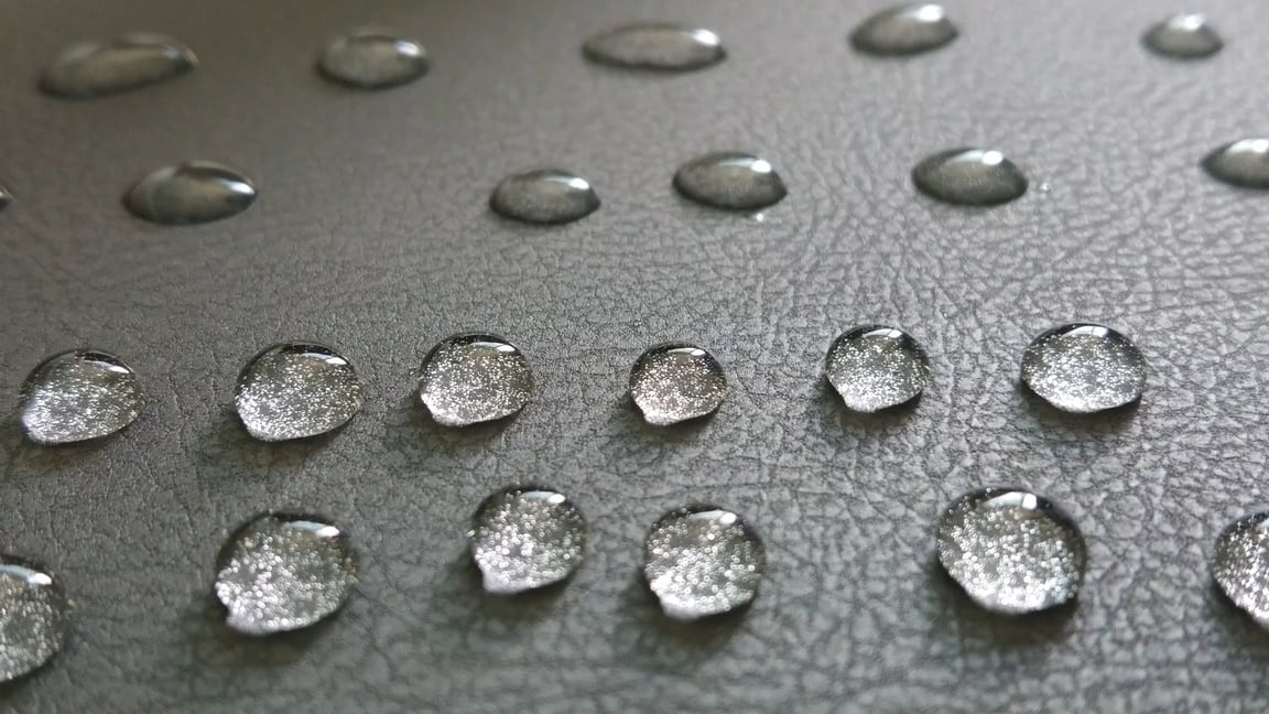
Semiconductor cleaning is different from general industrial cleaning. It involves removing microscopic contaminants such as metal ions, organic compounds, and submicron particles. If these remain on a part, they can alter electrical properties or damage circuits during processing. Standard cleaning methods are insufficient. Instead, manufacturers rely on specialised equipment and methods, including high-purity solvents, ultra-pure water, ultrasonic cleaning, and plasma-based techniques.
Failure to follow precise semiconductor cleaning standards can result in reduced yield or complete product rejection. This is particularly relevant during photomask cleaning, wafer carrier preparation, and tool maintenance. A single improperly cleaned part can compromise an entire batch, which costs time and resources. Therefore, every cleaning procedure must be validated, consistent, and traceable.
5 Key Methods Used in Semiconductor Parts Cleaning
- Ultrasonic Cleaning – High-frequency sound waves agitate a cleaning solution to remove particles from complex surfaces.
- Chemical Cleaning – Specialised solvents or acids dissolve inorganic or organic residues without damaging sensitive surfaces.
- Plasma Cleaning – This dry process removes surface contaminants using ionised gases and is effective for ultra-fine residues.
- Supercritical CO₂ Cleaning – This method uses supercritical carbon dioxide to remove particulates in a dry, residue-free process.
- Precision Rinsing and Drying – After cleaning, components undergo ultra-pure water rinsing and controlled drying to eliminate watermarks and residues.
Each method is selected based on the type of part, material composition, and level of contamination. Professional damage restoration services can expertly execute these methods to fully clean out the area. The cleaning environment, such as a certified semiconductor clean room, ensures these methods produce repeatable and high-quality results.
Challenges in Maintaining Cleanliness Standards
Semiconductor parts cleaning presents several challenges. Component designs continue to shrink, making them more sensitive to contamination. New materials and layered structures add complexity to the cleaning process. Additionally, the demand for shorter production cycles places pressure on cleaning teams to work faster without compromising precision.
Another challenge lies in monitoring and verification. Cleanliness must be measurable, utilising tools such as particle counters, surface analytics, and residue detection systems. The cleaning process must be optimised to remove contaminants while avoiding surface damage or chemical residue. Consistent training and process audits are also required to follow standards in high-volume manufacturing settings.
Conclusion
Precision in semiconductor parts cleaning directly affects product performance, reliability, and yield. As the industry pushes toward smaller nodes and more advanced materials, the importance of cleanroom environments and accurate cleaning methods will only increase. Clean parts contribute to fewer defects, more stable production, and longer equipment lifespan.
Protect your semiconductor assets with expert cleaning services. Contact BELFOR Restoration Services for professional support tailored to cleanroom standards.